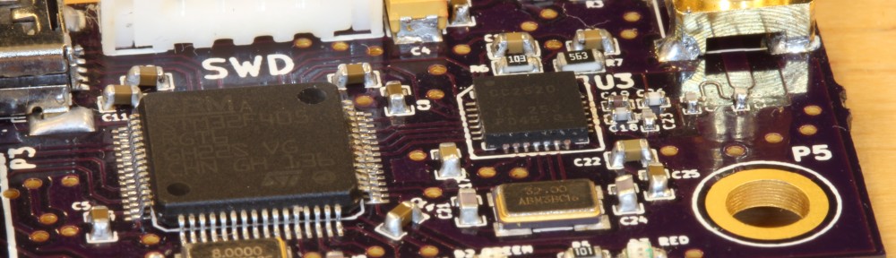
I have made a small PCB with an STM32F4 microcontroller and a TI CC2520 radio transceiver. There are many mote modules available already, but I wanted one optimized for performance as opposed to power consumption. I also wanted to try making a PCB with some RF-parts since I haven’t done that before.
These are the 2-layer PCBs ordered from OSHPark:
This is the schematic (a PDF can be downloaded here):
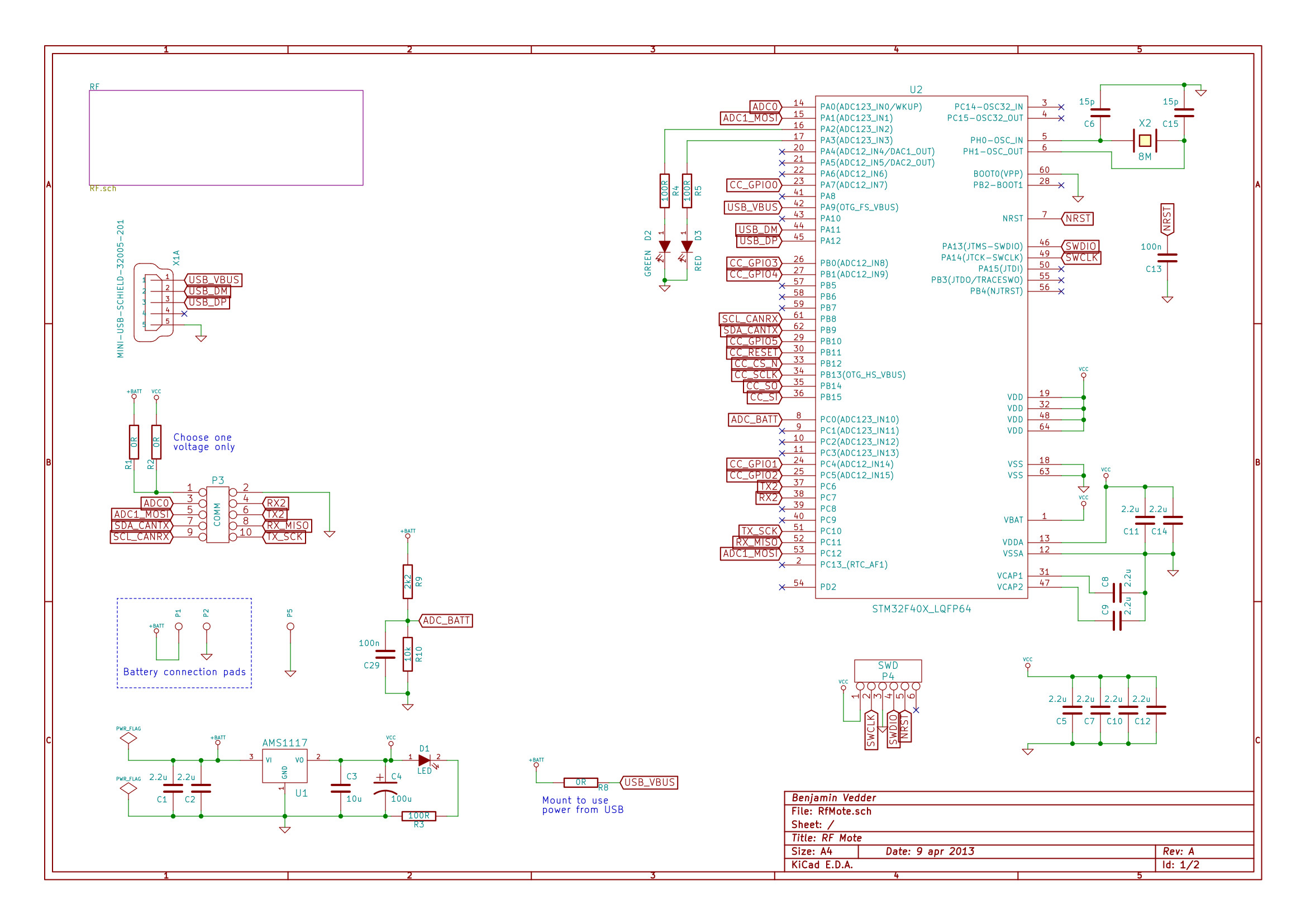
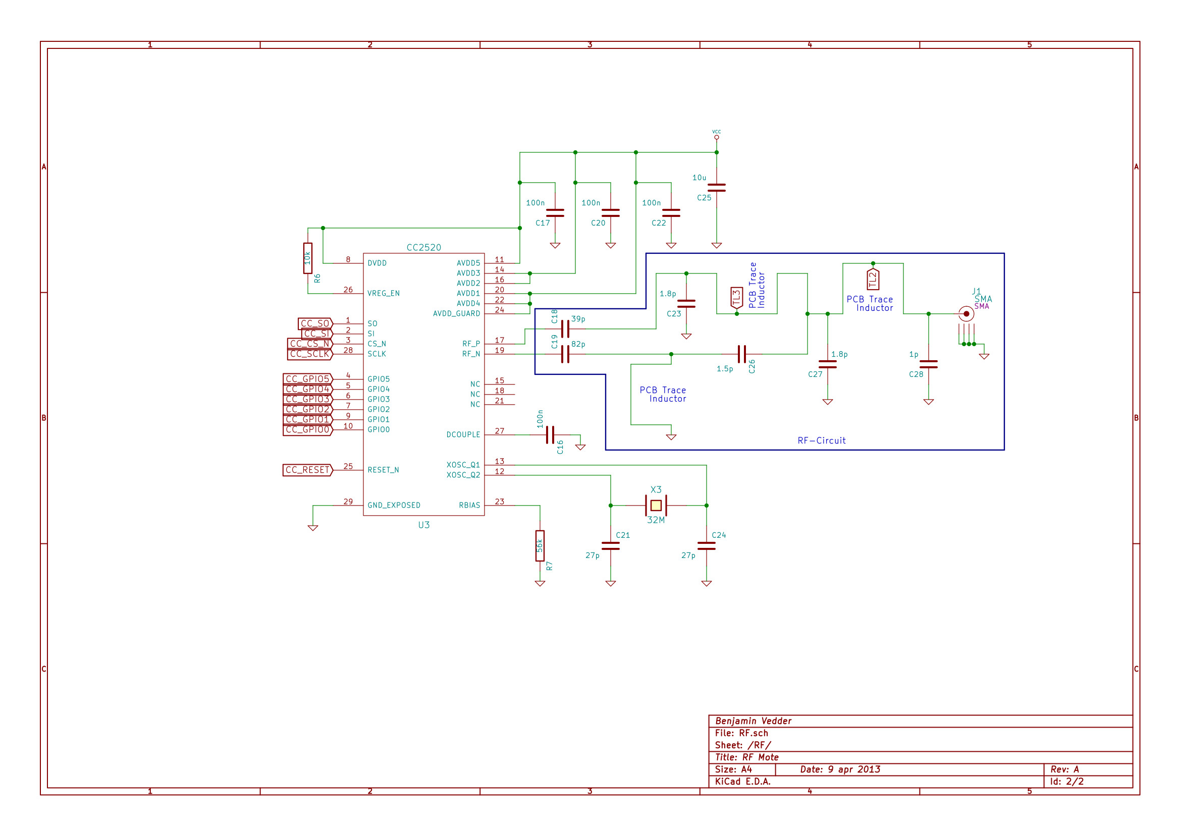
The KiCad files are here and the gerber files are here. All the components can be ordered from mouser. I also have an incomplete BOM with mouser numbers here.
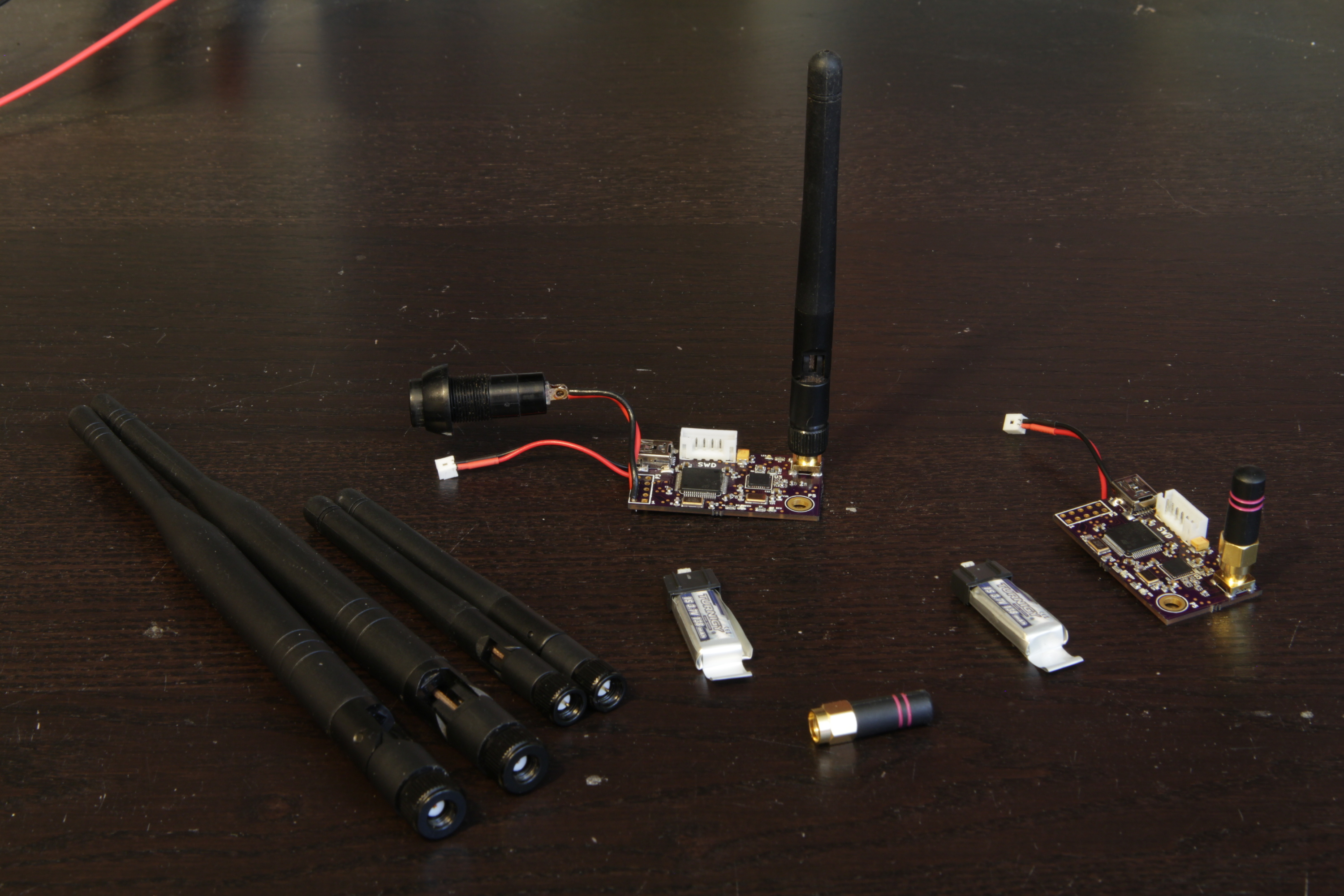
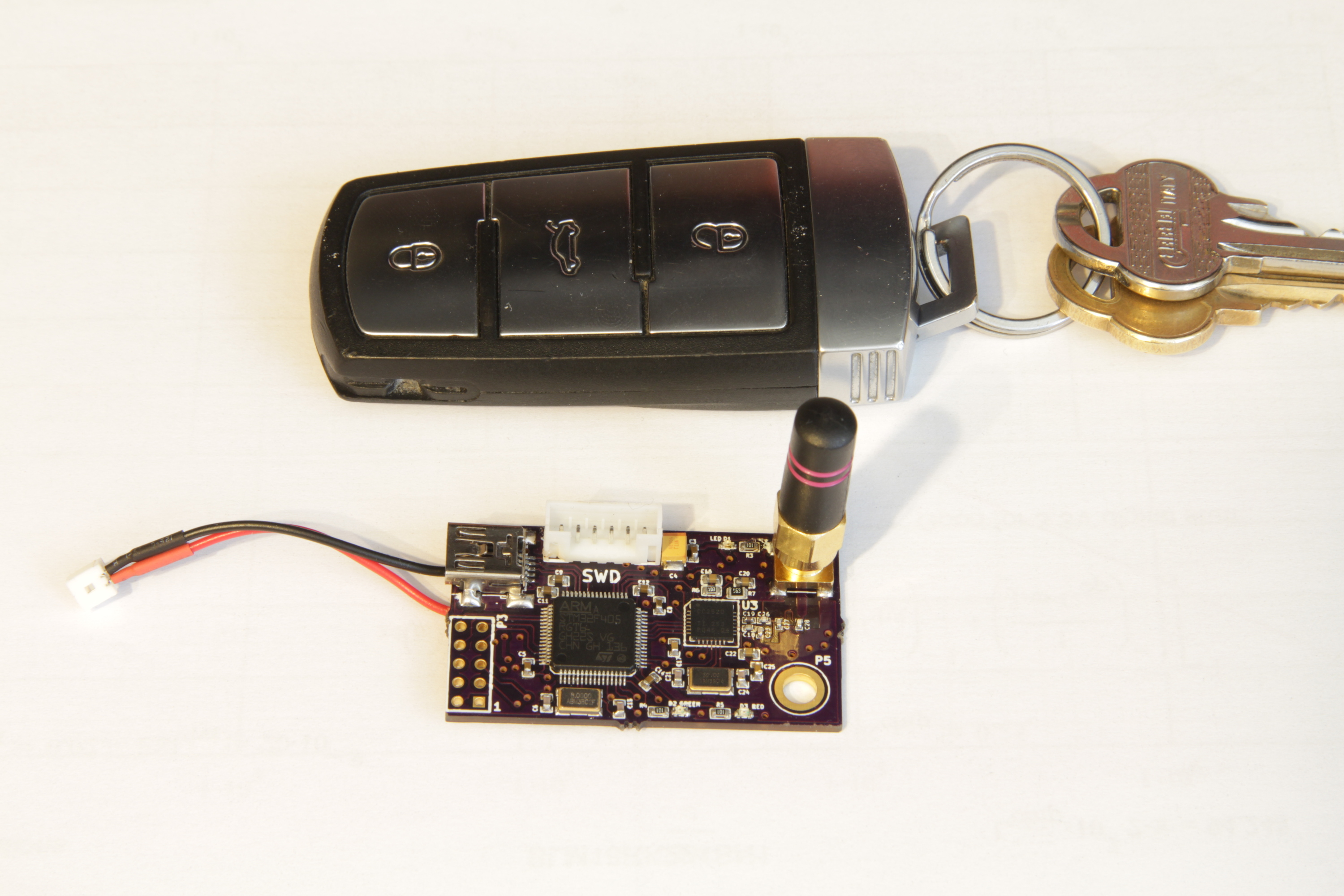
Here is one PCB next to my car key for size comparison:
Software
A Contiki port with instructions can be found here. A ChibiOS-version with instructions can be found here.
Uploading the program
The PCB has a SWD header with a 2mm-split microJST-connector. The STM32F4 discovery board works fine as a programmer and debugger. Just remove the jumpers from it and connect the SWD pins from the header to the RF-board (see the manual for the discovery board too see which pins are used). NOTE: Do not forget to connect the VCC pin to VDD on the discovery board, otherwise the programming will be un-reliable.
Range
This is the first time I make a PCB with RF-frequencies myself, so I’m sure I made some mistakes. Outdoors, the range was about 150m with 3dBi antennas. According to the datasheet of the CC2520 the range should be up to 400m, so the layout is most likely not perfect, although I tried to copy the reference design.
Update The new 0.8mm boards with the ground plane fixes and a few other fixes work a lot better. The measured output power is about 3.5 to 4.0 dBm, which is what it is supposed to be. I have updated the layout, schematic and production files on this page with these changes, so they should work quite well.
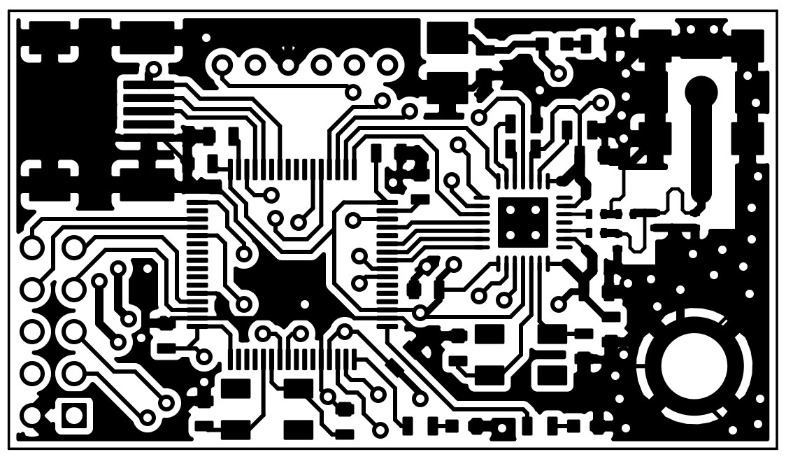
Here is what the front looks like:
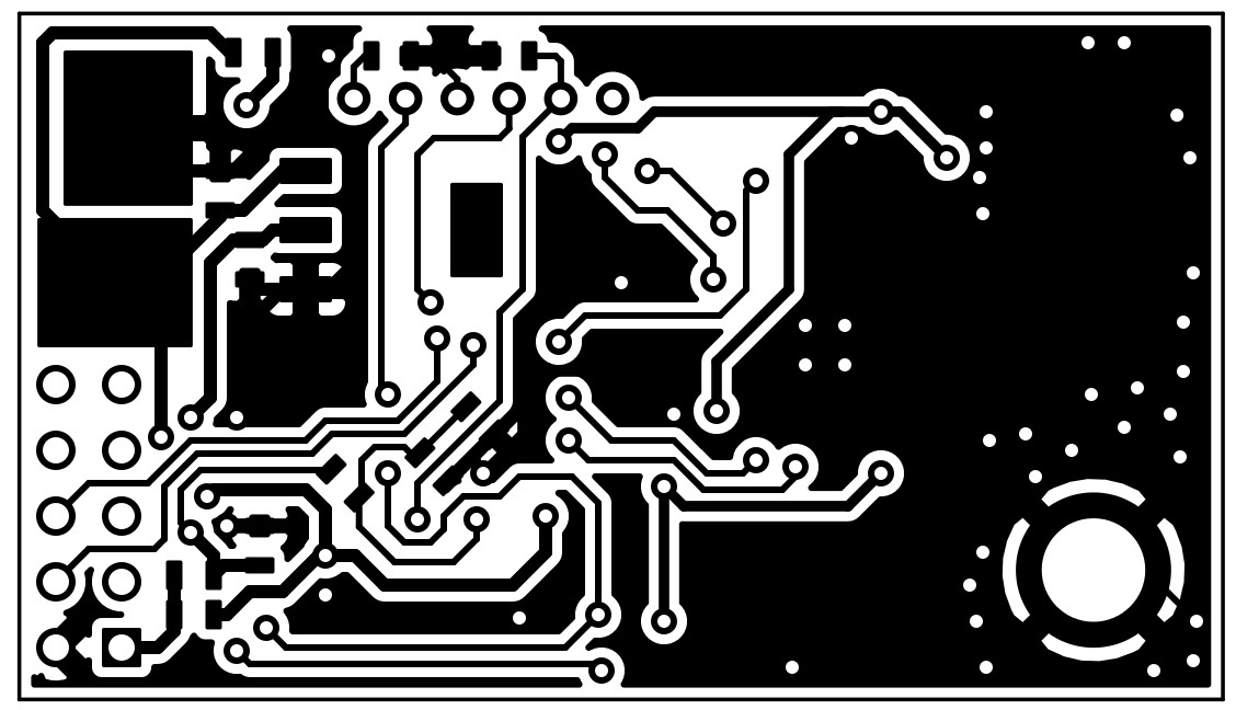
the back:
Also, one thing I discovered is that the tiny antennas in the pictures above are quite useless.
Update I made a few measurements, and apparently the output power is about 0.5dBm. I have read somewhere that the measured power from TIs reference is about 3dBm, so this layout is not that good. I have ordered new 0.8mm PCBs with more vias and a few ground plane fixes.
Improvements
I’m planning to make a new version of this board with the CC2591 power amplifier as well. This will hopefully improve the range a bit.
Feedback
Do you know RF? I would be glad to get some feedback on my design. Is there some obvious mistake that would make the range drop from 400m to 150m?
Update One problem might be that I used 1.6mm PCB thickness, the reference design uses 0.8mm. This changes the impedance of the trace to the SMA connector from 54 ohm to 77 ohm according to my calculation. The PCB trace inductors also change. How much does this matter?
Further reading
Adapting TI LPRF Reference Designs for Layer Stacking
Updates
2014-02-26
- I have made many improvements in my Contiki port recently. Make sure to use the latest version from gitub. You can find a description of it here.
- I have written a post about a ChibiOS-port for these boards here.
2013-06-11
- The 0.8mm boards are assembled and tested. The measured output power was 3.5 to 4.0 dBm. This is what it is supposed to be, so the RF-design seems to be in good shape. The range is also improved compared to the previous boards. NOTE: The design files that are provided above are the ones that worked with the 0.8mm PCBs, so if you want to build something similar you can base your design on them (on your own risk of course).
- I have started to port contiki to these boards, and made some progress. The USB-CDC library is ported and mapped with syscalls, so printf works for debugging. The LEDs also work. I still have to work on the radio part and make a few more tests. I will write a new post about the contiki port when it is done.
2013-04-09
- I read that the PCB thickness does matter here and here. My PCBs are 1.6mm thick and the ones in the reference design are 0.8mm. This will probably influence the PCB trace inductors.
- I Changed the layout a bit. The ground plane at the transceiver does not have as many cuts as before as I routed VCC another path. Also, there are more ground vias. The links above are updated, but the new design is not tested yet. I will try to order 0.8mm PCBs somewhere and test.
- I have measured the output power, and it is about 0.5dBm. I have ordered 0.8mm PCBs with the fixes fixes mentioned above. Hopefully this will increase the performance a bit.

Hi,
I want to use contiki on STM32F4Discovery board.
Do you have made an integration of this on eclipse ?
Best regards,
Pascal
Hi,
I am done with the porting, so the next step is to clean it up a little bit and upload it to github. This port is made for my RF-motes from this post, but it should run fine on the discovery board without the radio. The USB port should work right away, but you have to make a few minor changes to platform/stm32-bv/dev/leds-arch.c to use the LEDs.
I’m currently working on a post with a general description about my port and how to use it.
Have you done any more work on your Contiki port or posted it anywhere. I’m currently working on a board based upon the CC2520 and an STM32F1 series MCU so your port of Contiki would definitely be of interest to me, although it probably won’t work directly.
Yes, everything is working really well now and I have cleaned up most of the code. I am writing a post about my experiences and lesson learned from porting contiki right now, I will probably upload it this week if I have time along with contiki on github.
How do you solder the chip on the board? I always feel hard to solder crowding pins
First I put some solder on the pads, then I used a hot air soldering station.
Very nice! Bo Li – I have soldered these chips (STM32F4 in an LQFP-64) using a 1/32″ chisel tip soldering iron with very thin lead-free solder and tack flux from Chipquick. I clean with alcohol, apply thin strips of tack flux to the board, then seat the chip in the sticky tack flux. Then, I hold the chip in place with one end of a tweezer and solder a corner pin in place. Use Tip Cleaner if possible and keep the iron around 650F degrees. Tin the tip a bit more than will cover it with a thin layer and make sure that your angle is steep enough, so gravity pulls the solder down from the tip.
After doing one corner, I do the opposite corner, then do the ones in between. It really helps to have magnification since this chip is 0.5 mm pin density.
BTW, I cross-posted this over on http://www.reddit.com/r/stm32f4/
Pingback: ChibiOS on my cc2520+stm32f4 boards | Benjamin's robotics
>I would be really glad to get some feedback on my design. Is there some obvious
>mistake that would make the range drop from 400m to 150m?
Yes, there are, at least, two obvious mistakes:
1. The board must to be 4 layers, not two layers. Take a note: not “have to be”, but “must be”
2. all gnd has to be stitched by small vias. Randomly or chess pattern. I made my board with chess pattern. Check OSH Park for 4 layers requirements – they recently made minimal via requirements smaller than for 2 layers.
3. Better to have RF shield.
Last year I also made my first RF design for 915 MHz radio based on TI appnotes with small changes. My goal was to get maximum power with the same power. Datasheet promised 26.5 dBM. I did two sets of boards: 2 layers and 4 layers. My experiments with them showed +3 dBm for adding the RF shield and + 3dBm for switching from 2 layers to 4 layers board. The range changes were significant.
In your case RF Shield might be not needed because of low power (and I think you not care too much about FCC rules ;-)), but 4 layers and stitching vias you must have to get maximum performance. RF Shiled might help too.
Sorry, I did not notice from the firs look that you already have stitches 🙂
However, 4 layers are not there yet.
Thanks for the comments. I made some updates to the post, and with the latest PCBs I measured 4 dBm on the output, which is the same as TIs reference design has. TIs reference design actually has 2 layers, but a 0.5mm thick PCB. I got the full output power after ordering 0.5mm PCBs as well, so that was the main issue.
Hi, could you tell me 8Mhz ressonator reference?
Regards
On OSH Park there is this board?